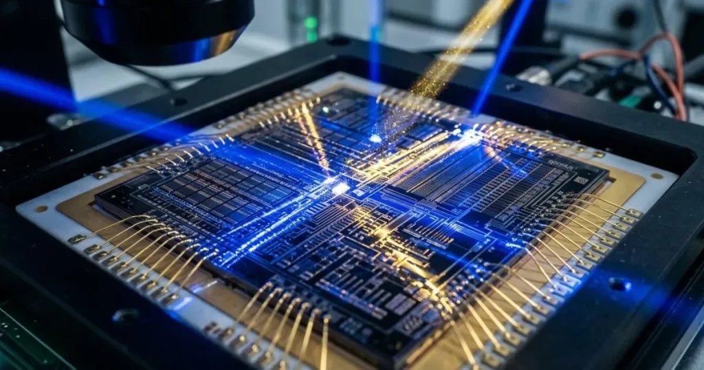
Every time you unlock your mobile phone, run a query to an artificial intelligence model, or send an instant message, billions of invisible microscopic switches flip in a fraction of a millisecond. They are transistors. For more than five decades, the microelectronics industry has followed a near-sacred maxim: constantly shrink them to cram an astronomical number of components onto a tiny silicon wafer. Yet the physics of matter is imposing an insurmountable boundary. How far can a transistor be reduced before quantum mechanics and thermodynamics prevent it from functioning?
The Atomic Limits of Modern Electronics
To maintain the unstoppable pace of cutting-edge computing capacity without thermally overwhelming today’s processors, microelectronic engineering urgently seeks alternatives to conventional silicon at the quantum frontier, developing innovative atomically thin two-dimensional semiconductors for the new digital era.
- The silicon limit: When the channel length falls below 5 nanometers, electrons begin to tunnel, causing massive leakage currents and overheating.
- The two-dimensional solution: Atomically thin tungsten disulfide semiconductors (WS_2) enable channels about 25 nanometers wide while preserving electrical control over the carriers.
- The AI energy challenge: Advanced processors for artificial intelligence consume up to 2.4 kW per chip, with more than half wasted as heat.
- The leap to three dimensions: The 3D architecture stacks layers of transistors upward like microscopic skyscrapers to multiply computational capacity.
What Is a Transistor and Why It Rules Our World
To grasp the physical size limit, we must first understand its essential nature. If you opened a laptop, a smartphone, or a modern appliance, you would see printed circuit boards populated with small black blocks: silicon microchips. If we magnified one of those chips a million times under a high-resolution microscope, we would uncover a complex network etched onto a silicon lattice. In that mesh reside the transistors.
A transistor is, in essence, a solid-state electronic switch with no moving mechanical parts. It operates by regulating the flow or cutoff of electric current through tiny voltage pulses. By opening and closing up to 4,000 million times per second in today’s commercial processors, these tiny components translate electrical flow into binary code: current flow is a logical “1,” and interruption is a “0.”
In Other Words: What They Do for Us (From the Largest to the Smallest)
In short, the transistor is the conceptual atom of all digital technology. Without it, the information society would simply not exist. To understand its practical utility directly and simply, it suffices to trace how we use them in daily life, from the grandest infrastructures to the most invisible devices:
At the largest scale (Supercomputers and AI servers): In the massive data centers that power AI language models or simulate planetary climate evolution on supercomputers, tens of billions of transistors operate simultaneously inside colossal processors. They are used to perform trillions of parallel mathematical calculations per second, enabling a machine to interpret natural language, analyze genomic sequences, or predict protein structures.
In the midrange (Personal computers, vehicles, and home technology): In a laptop, in the control unit of an electric vehicle, or in a smart TV, transistors manage everything from brake safety and GPS navigation to rendering 3D graphics and high-definition video encoding.
At the smallest scale (Smartphones, smartwatches, and medical sensors): In a pocket or on a wrist, billions of transistors packed into a tiny space process photos in real time, measure heart rate, or secure encrypted financial transactions. And at the far end of the scale, inside implantable pacemakers or biological diagnostic microchips, only a few thousand transistors regulate vital electrical impulses while consuming a negligible amount of energy for years.
The Atomic Frontier: 25-Nanometer Two-Dimensional Semiconductors
“Controlled switching in atomically thin semiconductors allows maintaining command over the electrons where conventional silicon begins to falter.” (Anton Persson, Chalmers University of Technology)
For half a century, silicon has reigned supreme in microelectronic technology. However, when the channel length through which electrons travel inside a silicon transistor drops below 5 nanometers, electrons start behaving according to quantum mechanics. Through the so-called tunneling effect, particles leak through insulating barriers, generating massive current leakage and overheating compared with the logic of quantum computers.
To overcome this physical limit, a research team led by Anton Persson (Chalmers University of Technology, Sweden) and Tara Peña (UCLA) published recently in Nature Nanotechnology has managed to construct nanoribbon transistors using two-dimensional tungsten disulfide semiconductors (WS_2). These 2D materials stand out for having a thickness of only one or a few atoms. By confining the current flow in an atomically thin layer (with a channel width of barely 25 nanometers, about 0.00025 the thickness of a human hair), researchers maintain electrical control over the electrons where traditional silicon fails.
The Heat Barrier and the Leap to the Third Dimension
“If we increase the number of transistors without making them more energy-efficient, the required power and the heat created will inevitably double.” (Prof. Suman Datta, Georgia Tech)
Reducing physical scale is not the sole concern of the industry; energy efficiency and heat dissipation pose challenges of equal magnitude. As warned by Professor Suman Datta from the Georgia Tech, stacking more transistors into the same footprint without improving each one’s energy efficiency will inevitably drive up the electricity bill and the heat to be expelled.
For example, the most advanced GPUs for data-center AI currently draw about 1.4 kilowatts of electrical power per chip, and future developments will push toward 2.4 kW, with more than half of that energy dissipated as residual heat. Therefore, microelectronic engineering seeks not only to shrink transistors on a flat two-dimensional surface but to grow upward through a three-dimensional architecture, stacking transistor layers on top of one another within the same microchip, in the same way skyscrapers are built to optimize urban space.
The Inevitable Evolution of Computing
Although in the lab conceptual proof-of-principle devices have been designed where a single atom controls the flow of electrons, the industry’s grand challenge remains to manufacture billions of these components with total reliability and commercially viable costs. The transition from traditional silicon toward atomically thin two-dimensional semiconductors, combined with three-dimensional stacking and thermal optimization, will ensure our devices continue to gain power and endurance in the AI era.